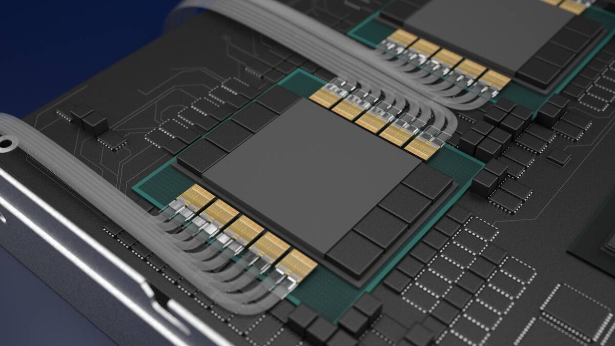
Optical I/O Advances: Bringing Photonics Closer to High-Performance Computing
Teh future of high-performance computing is rapidly evolving, and a key component of that evolution is optical input/output (I/O).Ayar Labs is making significant strides in this area, recently announcing a collaboration wiht Global Unichip Corporation (GUC) to accelerate the adoption of its photonic technology. This partnership aims to bridge the gap between promising prototypes and real-world, high-volume production.
The Promise of Optical I/O
Traditional electrical I/O is facing limitations as data demands surge. Optical I/O offers a compelling solution, promising substantially higher bandwidth, lower latency, and improved energy efficiency. You’re likely facing increasing pressure to deliver more performance with less power, and photonics is a critical path to achieving that.
Ayar Labs has already demonstrated the viability of its optical I/O technology through multiple prototypes.One notable example was developed in partnership with Intel and the Defense Advanced Research Projects Agency (DARPA).This demonstrates the technology isn’t just theoretical; it works.
Addressing the Challenges of Production
though, transitioning from successful prototypes to mass production presents substantial hurdles. Validating the technology for use with chips manufactured by companies like TSMC is a critical step. A failure in an optical I/O die could render a costly accelerator – potentially valued at $50,000 - unusable.
This is where GUC’s expertise comes into play. They will refine Ayar’s designs and validate them against established reference architectures. This validation is crucial for hyperscalers looking to integrate photonics into their future designs.
A Reference Flow for Scalability
The goal is to create a standardized design flow that high-volume manufacturers can readily access. this will significantly reduce the barriers to entry for integrating optical I/O. Many hyperscalers already prefer licensing intellectual property from companies like Broadcom and Marvell, rather than developing everything in-house. Ayar’s collaboration with GUC aims to provide a convenient pathway for these companies to adopt photonics.
According to igor Elkanovich, CTO of GUC, this joint design addresses key challenges including:
* Architectural considerations
* power efficiency
* Signal integrity
* Mechanical and thermal management
The result will be a robust, high-bandwidth, and power-efficient solution for your future needs.
Targeting Next-Generation Architectures
Initially,Ayar and GUC will focus on designs for XPU (extreme processing unit) architectures. They will leverage the UCIe-S and UCIe-A chiplet interconnect standards.These standards facilitate both package-level and die-to-die integration of Ayar’s optical I/O dies.
* UCIe-S: Enables integration at the package level.
* UCIe-A: Facilitates direct die-to-die communication.
Looking Ahead: When Will We See Results?
While the progress is exciting,widespread adoption won’t happen overnight. Ayar Labs anticipates that it will take approximately two years for the technologies to mature sufficiently for integration into accelerators in significant volumes. Though, this collaboration represents a major step forward in bringing the benefits of optical I/O to the broader high-performance computing landscape.
you can expect to see a growing emphasis on photonic solutions as the demand for faster, more efficient computing continues to escalate.This partnership positions Ayar Labs and GUC as key players in shaping that future.