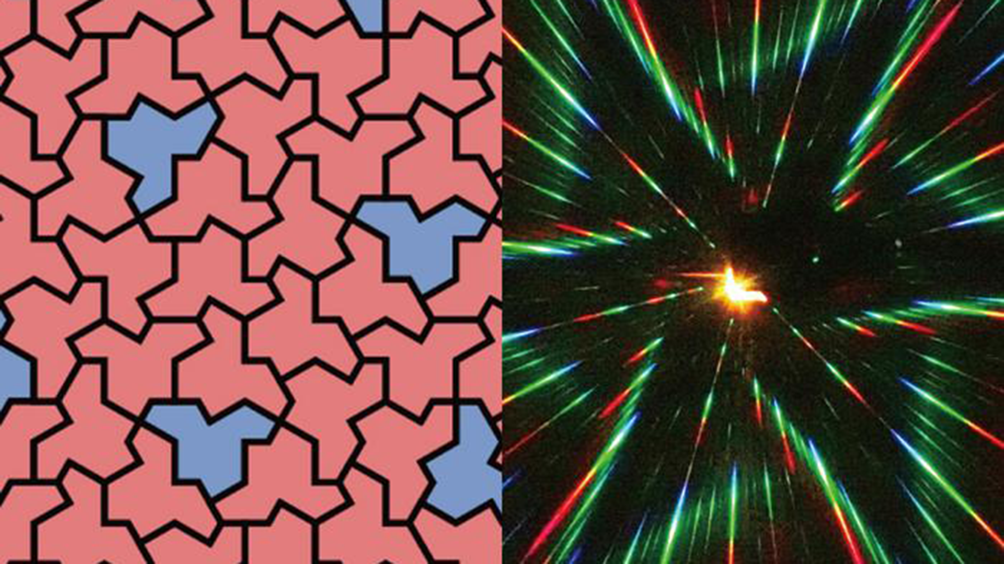
Physicists have constructed a novel photonic crystal using a 13-sided “einstein” tile shape, revealing that the engineered material bends light in ways regular crystals cannot. Published in the journal Nature Communications on July 29, the study demonstrates how researchers at the University of Tokyo arranged never-repeating geometric tile shapes into a pattern of nanoscale holes to manipulate light propagation. When researchers shined a laser at the surface, the structure produced a swirling, pinwheel-shaped scattering pattern that shifted depending on the rotational direction of the incoming light.
The research tackles a fundamental mathematical puzzle known as the “einstein problem,” which asks whether a single geometric shape can tile a flat surface infinitely without ever repeating its pattern. The term is a linguistic pun on the German phrase “ein stein,” translating to “one stone,” and bears no relation to physicist Albert Einstein. Decades prior, mathematician Roger Penrose demonstrated that a set of two distinct shapes could cover a surface aperiodically. However, a single-tile solution eluded researchers until 2023, when geometry enthusiast David Smith and his collaborators identified a 13-sided polygon known colloquially as the “Smith hat.”
Fabricating an Aperiodic Photonic Crystal
Yuto Moritake, an experimental physicist at the University of Tokyo, first encountered the hat tile in a popular science publication in 2024. Moritake specializes in photonic crystals, which are optical materials structured with microscopic arrangements designed to steer light for applications like lasers and optical sensors. While conventional photonic crystals rely on rigid, repeating grids, Moritake investigated what might happen if that regular grid was replaced with the hat tile’s aperiodic arrangement.
To fabricate the experimental chip, Moritake and his colleagues utilized electron beam lithography and etching. These precision manufacturing techniques punched hundreds of thousands of tiny holes—each measuring 100 nanometers in radius, or roughly 500 times thinner than a human hair—into a thin film of silicon nitride, a ceramic material widely used in computer chips. The array of holes spanned a silicon nitride chip approximately half a millimeter across, roughly matching the width of a standard pencil tip.
When the team directed a laser beam at the chip, the light diffracted into a distinct pinwheel-shaped configuration on a viewing screen. Moritake initially captured the colorful optical output using an iPhone camera set to long-exposure mode to record faint light over several seconds, followed by precise measurements using specialized scientific cameras. The resulting display featured well-defined bright spots known as Bragg peaks, which remained stationary regardless of where the laser struck the chip. This consistency confirmed that the structure possessed the long-range order characteristic of a quasicrystal—a material class whose structural units follow an orderly yet non-repeating arrangement, unlike the periodic lattices of table salt or diamond.
Chirality and Polarization Discovery
Because the hat tile lacks mirror symmetry—meaning its form cannot be superimposed onto its own reflection, akin to a human left and right hand—the resulting optical scattering pattern inherited this asymmetry, a property known to physicists as chirality. This structural asymmetry produced an unexpected optical response when tested with circularly polarized light, which travels while spinning either clockwise or counterclockwise like a corkscrew.
When Moritake tested the chip with both rotational directions of polarized light, he observed a subtle variance in how each orientation scattered off the material. Standard quasicrystals possessing mirror symmetry are generally incapable of producing this specific polarization-dependent disparity. “This structure can have some kind of circular polarization dependence,” Moritake noted, explaining that the polarization effect arose directly from the tile’s inherent asymmetry.
Future Applications in Optical Computing
Moritake aims to apply this aperiodic geometry to guide light traveling directly inside a photonic chip rather than observing light that merely reflects off the surface. Such advancements could eventually support optical communications and optical computing systems, which process and transmit data using photons instead of electrical currents.
Worth a look