Revolutionizing AI Hardware: Stanford-Led Team Achieves Breakthrough with Monolithic 3D Chip Design
Teh future of Artificial Intelligence (AI) hardware is taking shape, and it’s reaching up. A collaborative team of researchers from Stanford University,Carnegie Mellon University,the University of Pennsylvania,and MIT has unveiled a groundbreaking monolithic 3D chip design poised to dramatically accelerate AI processing and reignite domestic semiconductor innovation. This isn’t just an incremental enhancement; it’s a fundamental shift in how chips are built, offering performance gains previously considered unattainable.
The Challenge: Overcoming the Limits of 2D Chip Scaling
For decades, the semiconductor industry has relied on shrinking transistors to increase processing power – a principle known as Moore’s Law. however, this approach is reaching its physical limits. Continuing to miniaturize transistors is becoming increasingly expensive and complex, leading to diminishing returns. The demand for ever-increasing computational power, particularly for demanding AI applications, necessitates a new paradigm.
“we’ve hit a wall with conventional 2D scaling,” explains Professor H.-S.Philip Wong of Stanford University’s School of Engineering and principal investigator of the Northwest-AI-Hub.”To continue advancing AI capabilities, we need to think differently about chip architecture.”
Monolithic 3D Integration: A New architectural Approach
The team’s solution lies in monolithic 3D integration – a revolutionary technique that builds layers of circuitry directly on top of each other, creating a dense, vertically-oriented chip. This contrasts sharply with previous 3D chip attempts that involved stacking separately manufactured chips, which frequently enough suffered from limited connectivity and performance bottlenecks.
“We attacked it head-on by tightly integrating memory and logic and then building upward at extremely high density,” says a researcher at the university of Pennsylvania, drawing a compelling analogy: “It’s like the Manhattan of computing – we can fit more people in less space.”
This “monolithic” approach allows for significantly tighter integration and a far greater number of connections between layers. Crucially, the process utilizes relatively low temperatures, preventing damage to existing circuitry and enabling the creation of incredibly dense and efficient chips.
Domestic Manufacturing: A Strategic Imperative
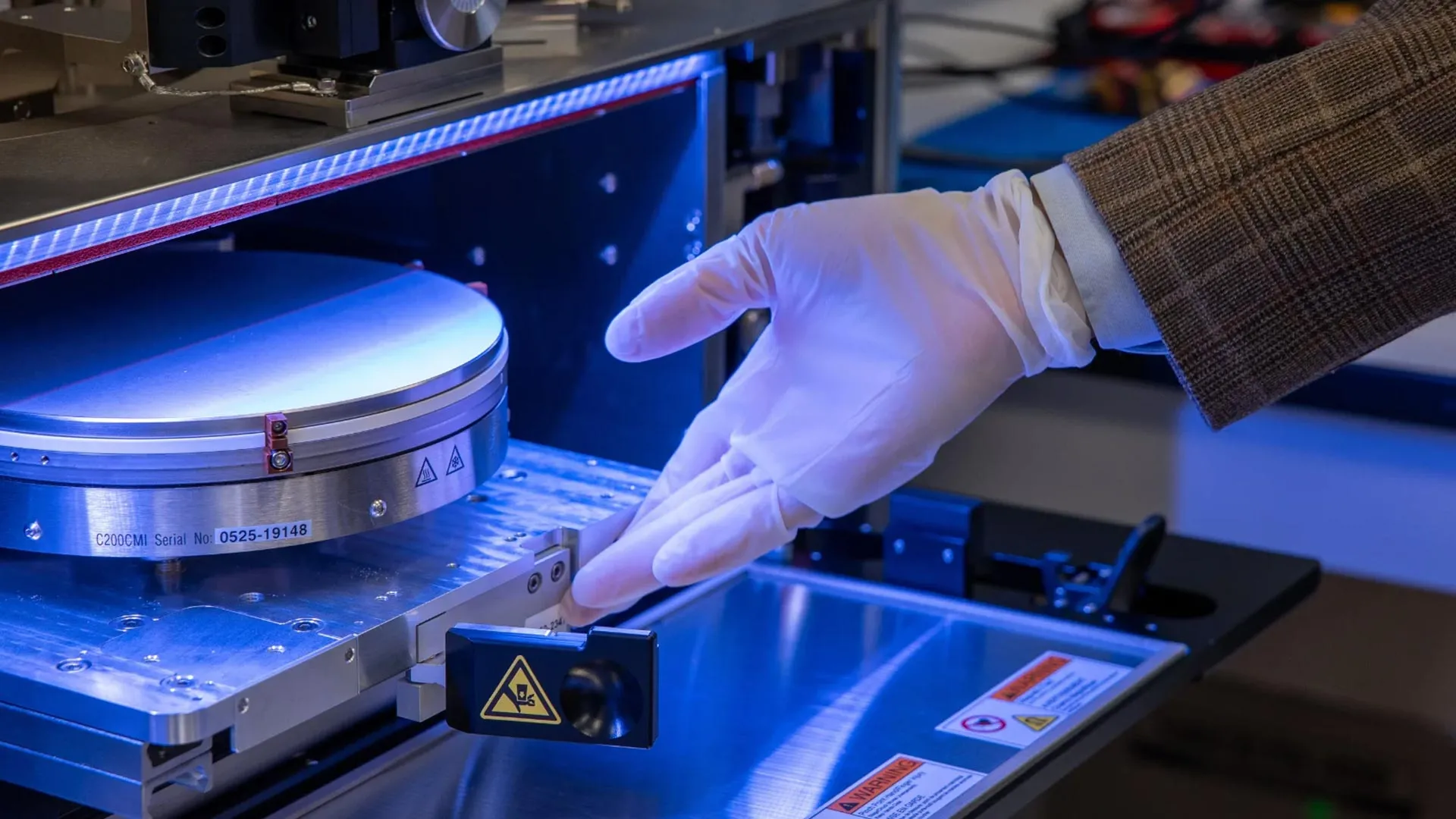
Beyond the technical achievement, this breakthrough is notable for its location of manufacture. The entire process was successfully executed in a U.S.-based commercial silicon foundry - SkyWater Technology in Bloomington, Minnesota.
“Turning a cutting-edge academic concept into something a commercial fab can build is an enormous challenge,” emphasizes Mark Nelson, Vice President of Technology Progress Operations at SkyWater Technology. “This shows that these advanced architectures aren’t just possible in the lab – they can be produced domestically, at scale, which is what America needs to stay at the forefront of semiconductor innovation.”
This capability is vital for national security and economic competitiveness, reducing reliance on foreign manufacturing and fostering a new era of American leadership in semiconductor technology.
Performance and Efficiency: A Quantum Leap for AI
Early hardware tests demonstrate the power of this new architecture. The prototype chip outperformed comparable 2D chips by a factor of four. Simulations predict even more ample gains as the design scales to include more layers, potentially achieving a twelve-fold improvement in performance on real-world AI workloads, including those based on Meta’s LLaMA model.
However, the benefits extend beyond sheer speed. the monolithic 3D design dramatically improves energy efficiency, measured by the Energy Delay Product (EDP). By minimizing the distance data needs to travel and providing numerous vertical pathways, the chip reduces energy consumption per operation – a critical factor for sustainable AI development. Researchers anticipate achieving 100 to 1,000-fold improvements in EDP, a game-changer for power-constrained applications.
Preparing for the Future: A New Generation of Semiconductor Engineers
The transition to monolithic 3D integration won’t be seamless. It requires a skilled workforce equipped with the knowledge and expertise to design, fabricate, and test these complex chips. Recognizing this need, initiatives like the microelectronics Commons California-Pacific-Northwest AI Hardware Hub (Northwest-AI-Hub) are actively investing in training the next generation of semiconductor engineers.
“Breakthroughs like this are of course about performance,” Wong concludes. “But they’re also about capability. If we can build advanced 3D chips, we can innovate faster, respond faster, and shape the future of AI hardware.”
Looking Ahead
This research represents a pivotal moment in the evolution of AI hardware. By demonstrating the feasibility and benefits of monolithic 3D integration, this team has laid the foundation for a new era of high-performance, energy-efficient computing, manufactured right here in the United States. The future of AI is not just about smarter algorithms; it’s about the innovative hardware that will power them.
Research Details:
*
Worth a look