MIT researchers and international collaborators have developed encapsulation epitaxy, a technique enabling wafer-scale growth of air-stable monolayer niobium diselenide.
Overcoming the Oxidation Barrier in Monolayer Superconductors
Two-dimensional superconductors hold immense promise for quantum computing and dense electronic circuits due to their flat, crystalline surfaces and microscopic dimensions. Yet, practical adoption has stalled because these ultrathin materials degrade immediately upon contact with ambient air. Niobium diselenide, or , stands out among these materials for its high kinetic inductance—a property allowing a tiny physical area to store substantial inductive energy. Until now, producing air-stable 2D superconductors required labor-intensive exfoliation to isolate microscopic flakes, because standard large-area growth attempts oxidized before protective layers could be applied.
Preserving Quantum Properties at Wafer Scale
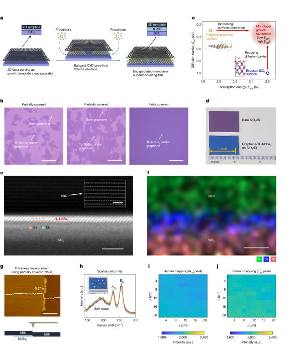
Because the superconducting film forms directly underneath the protective carbon lattice, it remains entirely shielded from ambient oxygen and moisture throughout the growth process.
Laboratory measurements confirm that these large-area sheets maintain their critical electronic characteristics after fabrication. The material exhibits a superconducting transition temperature of approximately 1 kelvin, fitting comfortably within the cryogenic environments required by superconducting quantum circuits to eliminate thermal noise. Furthermore, the films demonstrate an enhanced charge-density wave transition temperature near 177 kelvin. Because superconductivity and charge-density-wave order emerge from the same electronic system in niobium diselenide, the controlled interface provides an ideal platform for studying interacting quantum phases.
Integration into Working Superconducting Circuits
Creating a large sheet of material is only half the battle; engineers must also connect it to external wiring without triggering degradation. The MIT-led team developed specialized oxidation-free transfer protocols alongside a superconducting edge-contact method. By cutting the edges of the 1-nanometer-thick film inside a vacuum, researchers established direct electrical connections while keeping the active top surface fully protected.
Tests inside functional microwave circuits showed that the integrated material retained an impressive kinetic inductance of approximately 0.7 nanohenries per square.
“Emerging superconductors that are only a monolayer thick have a lot of potential. Thanks to our new process, they are no longer materials that can only be made at a very small scale. There are now exciting opportunities for scientists to study these materials, utilize them in circuits, and explore their practical applications.”
Xudong Sheldon Zheng, Department of Electrical Engineering and Computer Science, MIT
Future Directions and Alternative Substrates
Beyond niobium diselenide, the encapsulation epitaxy framework accommodates other protective overlayers, such as hexagonal boron nitride, and alternative underlying substrates like silicon nitride.
“We’ve taken a big step toward exploring both the science and applications of wafer-scale monolayer superconductors, which we can now grow in wafer scale or in even larger areas. There are a lot of directions we can go in the future.”
Sameia Zaman, Department of Electrical Engineering and Computer Science, MIT
With production hurdles cleared, the research team aims to extend the growth strategy to a wider family of monolayer quantum materials. Potential applications stretch past quantum processors into ultrasensitive quantum detectors tailored for advanced communications and cosmology.
Worth a look