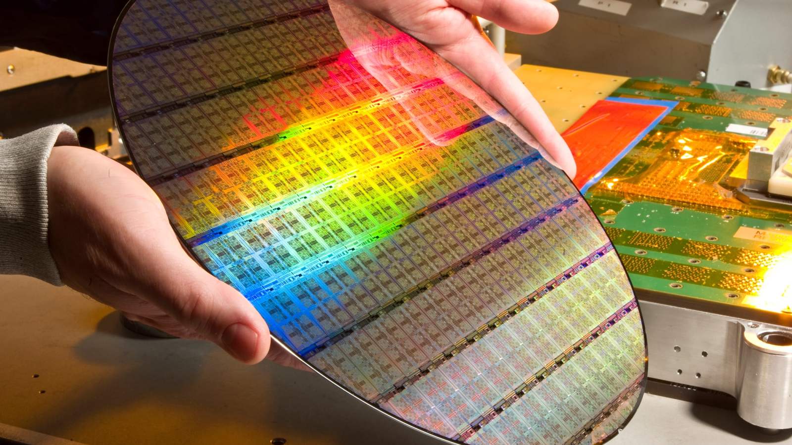
Samsung Electronics is reportedly securing a growing number of semiconductor manufacturing contracts from major global technology firms, including Tesla, BYD, Google, and AMD, as industry capacity constraints at TSMC create a supply chain bottleneck. As primary foundry competitors struggle to keep pace with the surging demand for high-performance computing and automotive-grade silicon, industry analysts observe that Samsung’s advanced manufacturing nodes are becoming a critical alternative for companies seeking to diversify their production pipelines.
The semiconductor industry is currently navigating a period of intense capacity utilization, particularly at Taiwan Semiconductor Manufacturing Co. (TSMC), which maintains a dominant market share in leading-edge logic fabrication. According to data provided by TSMC, the company has consistently operated at high capacity due to the explosive demand for artificial intelligence processors. This saturation has prompted fabless chip designers and automotive giants to re-evaluate their reliance on a single supplier, leading to increased interest in Samsung’s “Gate-All-Around” (GAA) transistor technology as a viable manufacturing path.
Strategic Shift in Automotive and AI Silicon
The automotive sector, specifically, has become a focal point for Samsung’s foundry expansion. BYD and Tesla have both intensified their efforts to internalize chip design, requiring reliable foundry partners to execute these complex architectures. Industry reports suggest that Samsung’s ability to provide automotive-grade certification for its 5nm and 4nm processes has been a key factor in these partnerships. As detailed by Bloomberg regarding foundry expansion strategies, Samsung is positioning its upcoming Texas facilities to serve these specific high-demand sectors, aiming to bridge the gap between design requirements and reliable, large-scale production.

Google’s involvement with Samsung is similarly rooted in the need for custom silicon for its Tensor processing units. By shifting production volumes to Samsung’s foundry, Google aims to maintain a consistent roadmap for its mobile and data center AI hardware. AMD, meanwhile, continues to balance its production load; while TSMC remains its primary partner for high-end CPU and GPU production, the company’s need to secure supply for broader product portfolios makes the utilization of Samsung’s mature and advanced nodes a strategic necessity to avoid inventory shortages.
Understanding the Capacity Bottleneck
The current supply environment is defined by a mismatch between the supply of Extreme Ultraviolet (EUV) lithography capacity and the rapidly rising demand for AI-specific chips. TSMC’s leadership has noted that the demand for AI-related silicon remains “real” and long-term, forcing them to prioritize high-margin orders for companies like NVIDIA. This prioritization inevitably displaces other clients, creating the “capacity gap” that Samsung is currently filling.

Samsung’s foundry division has been aggressively marketing its 3nm GAA process, which the company claims offers better power efficiency and performance compared to traditional FinFET architectures. According to a statement from Samsung Electronics, this transition is central to their effort to lure clients who are frustrated by the limited availability of advanced nodes elsewhere. For these clients, the risk of supply chain disruption is often a higher cost than the potential performance variance between different foundry processes.
Future Outlook and Market Impact
The long-term success of this strategy for Samsung depends on its ability to maintain high yields at its advanced nodes. While TSMC has historically held a lead in yield consistency, Samsung’s intensive investment in packaging technologies—specifically its Integrated Heat Spreader (IHS) and advanced 2.5D/3D packaging solutions—is designed to provide a comprehensive “turnkey” service for its clients. This approach is intended to simplify the supply chain for companies like Google and AMD, who prefer to work with partners that can handle both fabrication and advanced assembly.

Market observers expect that the next major update regarding foundry allocation will emerge during the upcoming quarterly earnings calls for these respective companies. Investors and industry participants are monitoring whether these partnerships will lead to a significant shift in market share for the foundry industry over the next 18 to 24 months. As production schedules for 2025 and 2026 are finalized, the visibility into these manufacturing commitments will clarify whether Samsung’s strategy will successfully challenge the current foundry market hierarchy.
Readers interested in the official progress of these facilities can monitor updates through the U.S. Securities and Exchange Commission (SEC) filings, which frequently disclose material supply agreements and capital expenditure projects for major technology firms. We encourage our readers to share their insights on how these foundry shifts might impact consumer electronics pricing and availability in the coming year.
Related reading
- Anthropic’s Mythos 5 Executes Real-World Supply Chain Attack in AI Safety Test
- Namuwiki Document Revision History 2026-08-05
- Google Pixel 11 Pro Leaks Reveal Price Hikes and HiLight Feature Ahead of Launch (archyworldys.com)
- Samsung Removes Smart TV Apps That Used Home Internet as Residential Proxies (time.news)