
Samsung Electronics is reportedly exploring a massive expansion of its semiconductor operations in Southeast Asia, with plans for a Samsung semiconductor packaging project Vietnam that could see an investment of up to $4 billion. The proposed project focuses on the establishment of a chip packaging and IC testing facility, marking a strategic move to deepen the company’s manufacturing footprint in the region.
The move comes at a critical juncture for the global electronics industry as chipmakers race to meet the surging demand for advanced semiconductors required for AI servers and a new generation of electronic devices. If finalized, this facility would represent a significant shift in Samsung’s global strategy, potentially becoming the company’s second overseas backend semiconductor site outside of South Korea and China, according to reports from DIGITIMES Asia.
While Samsung representatives have declined to comment on the matter, the Vietnamese government has indicated that discussions are underway. Vietnam’s finance ministry confirmed it is currently working on a memorandum of understanding (MoU) with Samsung regarding a semiconductor-related project, signaling a high level of coordination between the tech giant and the host nation.
The $4 Billion Blueprint: Phased Investment and Scope
The scale of the proposed investment is substantial, with reports indicating a total outlay of approximately US$4 billion. According to sources familiar with the matter, the project is expected to be implemented in stages rather than as a single lump-sum investment. The initial phase would reportedly consist of a US$2 billion tranche to kickstart the facility’s development.
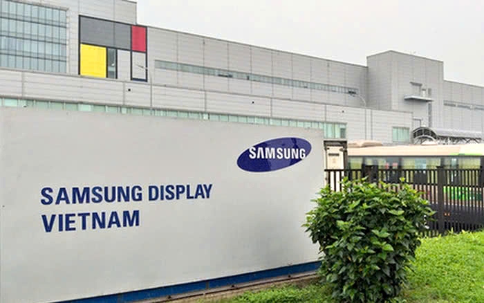
The facility is planned for construction in northern Vietnam, a region that has already become a hub for Samsung’s manufacturing activities. Unlike “front-end” fabrication, where the actual silicon wafers are created, this project focuses on “backend” operations. This includes semiconductor packaging—the process of encasing the chip in a protective shell and connecting it to the outside world—and IC (Integrated Circuit) testing, which ensures the chips function correctly before they are shipped to customers.
By establishing a dedicated backend assembly and test-related facility, Samsung can better integrate its supply chain, reducing the logistical complexity of moving wafers between different countries for final processing and quality assurance.
Diversifying the Global Semiconductor Supply Chain
The push into Vietnam is more than just a capacity increase; it is a strategic diversification of the semiconductor supply chain. For years, the industry has been heavily concentrated in a few geographic hubs. By expanding its backend capabilities into Vietnam, Samsung reduces its reliance on existing sites in South Korea and China.
This diversification is particularly urgent given the current technological climate. The rise of artificial intelligence has created an unprecedented need for high-performance chips. AI servers, in particular, require advanced packaging techniques to handle the massive data throughput and power requirements of modern GPUs and AI accelerators. Enhancing backend capacity is essential for Samsung to remain competitive against other global chipmakers who are similarly accelerating their spending to preserve pace with AI demand.
Vietnam has emerged as an attractive destination for this investment due to its existing relationship with Samsung and its growing role in the global electronics ecosystem. The country’s ability to attract large-scale foreign direct investment in high-tech manufacturing makes it a logical choice for a project of this magnitude.
Current Status and Government Coordination
Despite the detailed reports regarding the investment figures and the location, the project has not yet reached a final agreement. Sources indicate that while discussions are ongoing, no memorandum of understanding (MoU) has been finalized at this stage. The Vietnamese finance ministry is actively involved in the process, working to structure the agreement to support the semiconductor manufacturing project.
The lack of a formal announcement from Samsung is typical for projects of this scale, where negotiations over land, tax incentives, and infrastructure support can take considerable time. However, the confirmation from the Vietnamese government that they are working on a semiconductor-related MoU provides a strong indication that the project is moving forward in a formal capacity.
Key Project Details at a Glance
| Detail | Reported Specification |
|---|---|
| Total Estimated Investment | US$4 Billion |
| Initial Funding Tranche | US$2 Billion |
| Primary Location | Northern Vietnam |
| Facility Type | Backend (Packaging and IC Testing) |
| Current Stage | Discussions / MoU Development |
As the industry continues to evolve, the outcome of these negotiations will be a key indicator of how Samsung intends to navigate the geopolitical and economic pressures of the chip war. The establishment of a major backend hub in Vietnam would not only bolster Samsung’s operational resilience but also elevate Vietnam’s status within the global semiconductor hierarchy.
The next critical milestone for this project will be the official signing and announcement of the memorandum of understanding (MoU) between Samsung and the Vietnamese government, which will provide definitive details on the project’s scope, timing, and official investment commitments.
Do you believe Southeast Asia will become the next major hub for semiconductor backend processing? Share your thoughts in the comments below or share this article with your network.