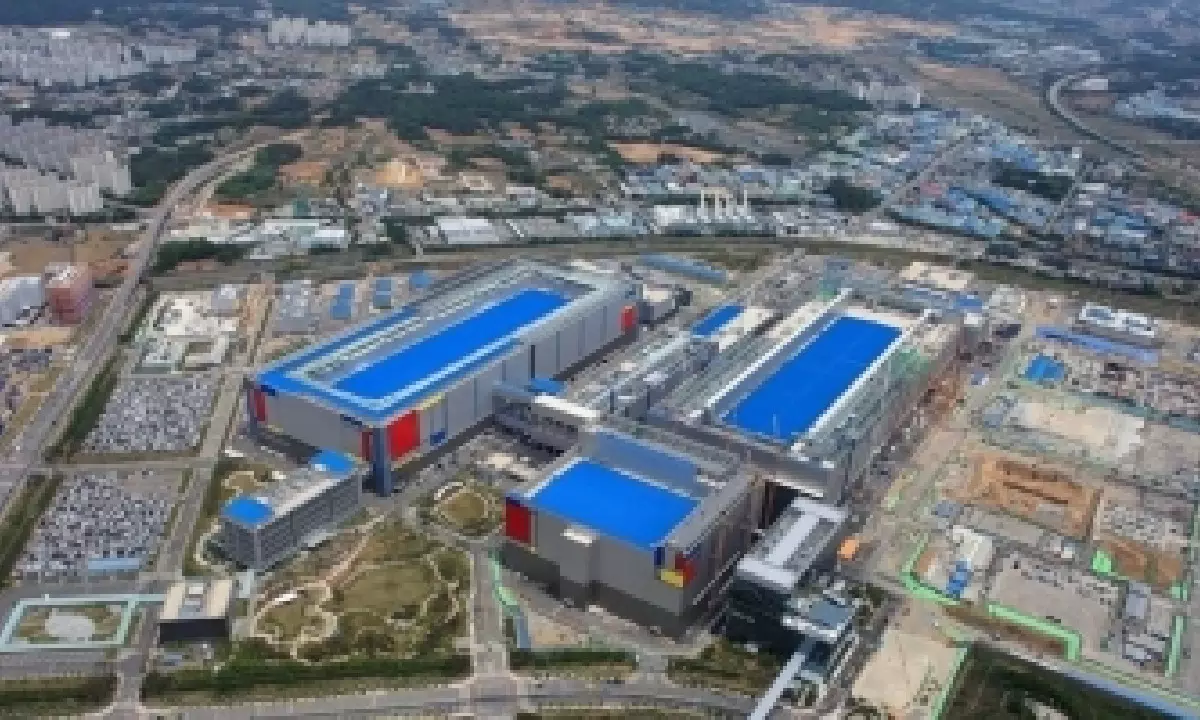
Samsung Electronics has confirmed plans to accelerate the timeline for its semiconductor manufacturing facility in Yongin, South Korea, aiming to begin operations by 2029. This strategic shift moves the production start date forward, reflecting the company’s ongoing efforts to bolster its domestic chip manufacturing capacity amidst intensifying global competition in the semiconductor sector. According to Reuters, the adjustment is part of a broader push by the technology giant to secure its supply chain and maintain its market position.
Strategic Expansion in the Semiconductor Cluster
The Yongin site is a central component of South Korea’s “Mega Semiconductor Cluster,” a massive industrial project located south of Seoul. The facility is designed to serve as a hub for advanced chip production, focusing on high-bandwidth memory (HBM) and next-generation logic chips essential for artificial intelligence and high-performance computing. As reported by Bloomberg, the 2029 target represents an effort to align production capacity with the surging demand for AI-related hardware, which has become a primary driver for global semiconductor growth.

The development of the Yongin cluster is supported by government initiatives aimed at strengthening the domestic semiconductor ecosystem. By consolidating research, design, and manufacturing in a single geographic area, Samsung expects to achieve greater operational efficiency and faster iteration cycles for its silicon products. This infrastructure development is critical for the company as it navigates the complexities of the current geopolitical landscape and the rising costs of advanced lithography equipment.
Market Context and Competitive Pressures
Samsung’s decision to expedite its timeline comes at a time when the semiconductor industry is experiencing significant volatility. Rival manufacturers, including TSMC and SK Hynix, are also aggressively expanding their production footprints to address the AI boom. The industry-wide push for localized manufacturing in regions like the United States, Europe, and Japan has prompted South Korean firms to further invest in their home base to ensure long-term competitiveness.

From an engineering perspective, the transition to 2029 requires precise coordination of construction, equipment installation, and workforce training. The facility is expected to utilize the latest in extreme ultraviolet (EUV) lithography, a technology that is essential for producing the ultra-fine circuit patterns required for modern processors. The investment scale is substantial, with the South Korean government providing support through infrastructure grants and regulatory streamlining to ensure the project remains on schedule, as noted in reports from The Korea Times.
What This Means for the Global Supply Chain
For global stakeholders, the acceleration of the Yongin plant signals a potential increase in the availability of high-density memory products toward the end of the decade. As AI models grow in complexity, the reliance on specialized memory chips—specifically HBM—has intensified. By bringing the Yongin facility online earlier, Samsung aims to mitigate potential supply shortages that could otherwise constrain the growth of the broader technology sector.
Furthermore, this expansion is an indicator of how major technology firms are responding to the demand for “sovereign” chip production. By strengthening its domestic capacity, Samsung is effectively hedging against potential supply chain disruptions caused by trade tensions or regional instability. The success of this project will likely depend on the company’s ability to manage the logistics of large-scale construction while simultaneously maintaining its existing production lines at other global sites.
Future Milestones and Operational Updates
While the 2029 date provides a clear target, the project remains subject to ongoing construction progress and the successful integration of complex manufacturing equipment. Interested parties and investors can monitor official announcements from the Samsung Electronics Investor Relations portal for updates regarding capital expenditure and construction milestones.

The next major checkpoint for the project will likely involve the installation of the primary manufacturing tools, which usually occurs in the 12 to 18 months preceding full-scale production. As the company moves toward these milestones, further details regarding the specific chip architectures to be produced in Yongin are expected to be disclosed. We will continue to track the development of the Yongin cluster as more information becomes available. Readers are encouraged to share their insights on the future of semiconductor manufacturing in the comments section below.
Worth a look