For years, scientists have been captivated by the potential of atomically thin semiconductors—materials just a single layer of atoms thick that promise to revolutionize the future of electronics and optics. However, these materials face a fundamental physical hurdle: they are simply too thin. Because there is so little material for light to interact with, the resulting light emission and frequency conversion are often too weak to be practical for real-world applications.
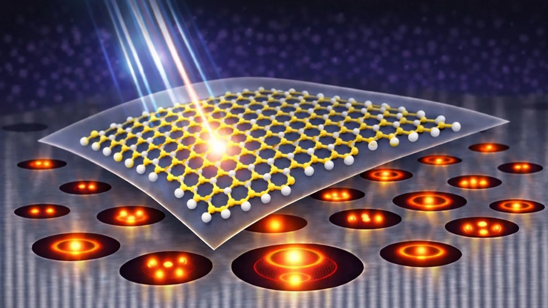
A research team at the Australian National University (ANU) in Canberra has developed a sophisticated solution to this limitation. Rather than attempting to alter the two-dimensional material itself, the researchers have reimagined the space beneath it. By creating a hybrid photonic platform that uses Mie void resonators for semiconductors, the team has found a way to “trap” and concentrate light exactly where it is needed most.
This breakthrough, detailed in a study published in the journal Advanced Photonics, involves coupling a monolayer of tungsten disulfide (WS₂) to subwavelength air cavities, known as Mie voids, which are carved into a high-index crystal of bismuth telluride (Bi₂Te₃). The result is a system that significantly boosts light-matter interactions, potentially clearing the path for more efficient quantum optics, sensing technologies, and on-chip light sources.
Redefining the Space Beneath the Surface
To understand the significance of this development, it is necessary to gaze at how light is typically managed in nanotechnology. Conventional dielectric nanoresonators are designed to trap light inside solid materials, such as silicon. While this approach is effective for many applications, it has a critical flaw when dealing with atomically thin materials: it concentrates the optical fields inside the solid host, away from the surface where the thin semiconductor resides.

traditional resonators often struggle when the host material absorbs light, which can damp resonances and reduce the overall strength of the optical field. The ANU team’s approach flips this logic on its head by using “empty space” as the resonator. By carving nanoscale air cavities—the Mie voids—into a bismuth telluride substrate, the researchers have created a platform that concentrates light at the interface between the void and the material.
According to reports on the development, these Mie voids allow for the direct visualization of localized optical modes and strongly enhance both light emission and nonlinear optical signals via optics.org. By reshaping the environment rather than the semiconductor, the researchers have overcome the inherent limitation of the material’s extreme thinness.
The Power of Tungsten Disulfide and Excitons
The material at the center of this research, tungsten disulfide (WS₂), is a member of a class of semiconductors that are promising for future photonic technologies. Despite being only one atom thick, WS₂ hosts what are known as excitons—tightly bound pairs of electrons and holes that interact strongly with light.
These excitons allow the material to efficiently generate new wavelengths of light through nonlinear optical processes, such as second-harmonic generation. This ability to manipulate light frequencies is essential for creating the next generation of on-chip light sources and highly sensitive sensors. However, without the enhancement provided by the Mie voids, these effects are often too faint to be useful in integrated circuits.
By placing the WS₂ monolayer directly on top of the bismuth telluride’s air cavities, the hybrid platform ensures that the excitons are subjected to an intensified optical field. This coupling “supercharges” the semiconductor, allowing it to shine brighter and interact with light more vigorously than it could in a vacuum or on a standard flat substrate via SciTechDaily.
Implications for Quantum Optics and Sensing
The ability to program and control light at the nanoscale has profound implications for several high-tech sectors. In the realm of quantum optics, the ability to strongly couple light to a single layer of atoms is a prerequisite for developing quantum bits (qubits) and single-photon sources, which are the building blocks of quantum computing.
In the field of sensing, the enhanced nonlinear optical signals provided by the Mie void platform could lead to detectors capable of identifying chemical or biological markers at much lower concentrations than currently possible. Because the light is concentrated at the particularly surface of the device, the system is exquisitely sensitive to changes in the surrounding environment.
the development of on-chip light sources is a primary goal for the semiconductor industry. Currently, many optical components must be integrated onto chips using complex and expensive packaging. A platform that allows atomically thin materials to generate strong optical signals directly on a substrate could lead to more compact, energy-efficient photonic integrated circuits (PICs) via phys.org.
Key Takeaways of the Hybrid Photonic Platform
- The Challenge: Atomically thin semiconductors like tungsten disulfide (WS₂) are too thin to interact strongly with light on their own.
- The Solution: Researchers at the Australian National University created “Mie voids”—subwavelength air cavities carved into a bismuth telluride (Bi₂Te₃) substrate.
- The Mechanism: Unlike traditional resonators that trap light inside a solid, Mie voids concentrate the optical field at the surface, where the semiconductor sits.
- The Result: This configuration enhances light emission and nonlinear optical signals, making the material more effective for photonic applications.
- Potential Uses: The technology is applicable to quantum optics, high-sensitivity sensing, and the development of on-chip light sources.
As the industry moves toward smaller, faster, and more energy-efficient devices, the ability to manipulate light at the atomic scale will be paramount. The work published in Advanced Photonics demonstrates that sometimes the most effective way to improve a material’s performance is not to change the material itself, but to carefully engineer the void around it.
While this research represents a significant step forward in hybrid photonic platforms, the next phase of development will likely focus on scaling these Mie void arrays for commercial manufacturing and testing their stability in diverse environmental conditions.
We invite our readers to share their thoughts on the future of photonic integration in the comments below. Do you believe atomically thin semiconductors will replace traditional silicon in optical computing?
Keep reading