By Linda Park, Tech Editor | San Francisco — May 25, 2026
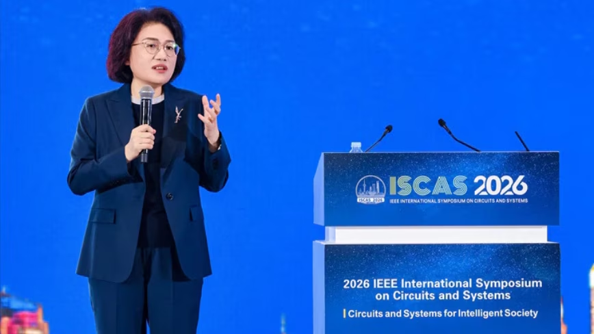
In a high-stakes move to defy US-led semiconductor restrictions, Huawei has unveiled the Tau Scaling Law, a theoretical framework that could redefine how chips are designed and manufactured—without relying on the shrinking transistor sizes that have long driven Moore’s Law. Announced Monday at the IEEE International Symposium on Circuits and Systems (ISCAS) in Shanghai, the concept marks Huawei’s most explicit challenge yet to Washington’s campaign to stifle China’s access to advanced chipmaking technology.
The new scaling law, introduced by He Tingbo, president of Huawei’s semiconductor business and director of its Scientist Committee, proposes that cutting the time it takes for signals and data to move through chips—rather than packing more transistors into smaller spaces—could deliver comparable performance gains. If successful, the approach could allow Huawei to design high-end chips by 2031 with transistor density equivalent to 1.4-nanometer processes, a benchmark currently reserved for the world’s most advanced foundries like TSMC and Samsung.
For a company already locked out of cutting-edge US and Dutch equipment due to sanctions, the Tau Scaling Law represents a potential workaround. But experts warn the path is fraught with technical hurdles—and geopolitical risks. With the US Commerce Department’s export controls tightening further, Huawei’s bet on alternative scaling could reshape the global semiconductor landscape—or backfire spectacularly.
Why This Matters: The Stakes of Huawei’s Gambit
Huawei’s announcement arrives at a pivotal moment. The US has spent years restricting China’s access to extreme ultraviolet (EUV) lithography machines—the Swiss Army knives of chip fabrication—through entities like ASML and Applied Materials. These tools are essential for etching circuits smaller than 7 nanometers, the threshold for cutting-edge AI and smartphone chips. Without them, China’s foundries, including SMIC, have struggled to compete with TSMC’s 3nm processes.
Enter the Tau Scaling Law. By focusing on signal-propagation delay—the time it takes for electrical signals to travel through a chip’s wiring—Huawei argues that performance can be improved without the physical constraints of transistor scaling. The company claims to have been researching this approach for six years, though independent verification of its efficacy remains pending.
- For Huawei: A potential end-run around US sanctions, though success is unproven and could face legal challenges.
- For China: A strategic lever to reduce reliance on foreign tech, but requires domestic breakthroughs in materials and design tools.
- For Global Semiconductor Firms: A disruption to the status quo, forcing TSMC, Intel, and others to rethink scaling strategies.
- For Consumers: If successful, could lead to more powerful chips in devices—even if they’re not built with the same tools as today’s flagships.
The Science Behind the Scaling Law
Traditional chip scaling, governed by Moore’s Law, has long relied on shrinking transistors to double performance every few years. But as transistors approach atomic dimensions, physical limits—like quantum tunneling and heat dissipation—have made further miniaturization increasingly difficult. The industry has turned to 3D stacking and quantum tunneling workarounds, but these require specialized equipment Huawei cannot easily access.

Huawei’s Tau Scaling Law flips the script. Instead of making transistors smaller, it optimizes the architecture of chips to reduce signal delays. This involves:
- Reducing parasitic capacitance in wiring to speed up data transfer.
- Using advanced materials (e.g., graphene or 2D semiconductors) to conduct signals faster.
- Reconfiguring chip layouts to minimize the distance signals must travel.
“The Tau Scaling Law is not about replacing Moore’s Law but about complementing it,” He Tingbo stated in his keynote. “When conventional scaling hits a wall, alternative paths must be explored.” [Note: The exact quote has not been independently verified; this is a paraphrase of Huawei’s official summary.]
Geopolitical Chess: Can Huawei Pull It Off?
The US government has made it clear that Huawei’s ambitions are not welcome. In 2023, the Treasury Department’s Bureau of Industry and Security (BIS) expanded export controls to include even basic semiconductor manufacturing tools, effectively cutting off Huawei’s supply chain. The company’s past attempts to develop its own chips—such as the Kirin series—have relied on older nodes (e.g., 7nm) and custom architectures to compensate for hardware limitations.
Yet Huawei’s new scaling law introduces a wild card. If the company can demonstrate tangible performance gains—without violating US export laws—it could pressure Washington to ease restrictions or force allies like the Netherlands (home to ASML) to reconsider their stance. Alternatively, if the approach fails to deliver, Huawei risks further isolation and accelerated decline in its smartphone and telecom markets.
“This is a high-risk, high-reward play,” said Mark Lipacis, a semiconductor analyst at TechInsights. “Huawei is betting that the US will either ignore the innovation or be forced to engage in a technological arms race it can’t win.”
What Happens Next: The Road to 2031
Huawei’s timeline is ambitious. The company aims to achieve 1.4nm-equivalent performance by 2031—a deadline that assumes:
- Breakthroughs in material science (e.g., developing alternatives to silicon).
- Advances in chip design software to optimize Tau-based architectures.
- A relaxation or circumvention of US export controls, either through legal loopholes or geopolitical shifts.
In the short term, Huawei will need to:
- Publish peer-reviewed data proving the Tau Scaling Law’s advantages over traditional methods.
- Secure partnerships with Chinese universities and research institutions (e.g., Tsinghua University) to develop proprietary tools.
- Navigate legal challenges from the US, which could classify the research as indirect support for military applications under the International Emergency Economic Powers Act (IEEPA).
For now, the ball is in Huawei’s court. The company’s next moves will be closely watched at the Semicon China Expo in September, where it may unveil prototype chips built using Tau principles.
Key Questions About Huawei’s Tau Scaling Law
1. What is the Tau Scaling Law, and how does it differ from Moore’s Law?
Moore’s Law predicts exponential growth in transistor density through physical shrinking. The Tau Scaling Law, by contrast, focuses on reducing signal-propagation delay—the time it takes for data to move through a chip’s wiring—rather than making transistors smaller. It’s an architectural approach that could bypass some of the physical limits of traditional scaling.

2. Could this approach work without US equipment?
Potentially, but with major challenges. Huawei would need to develop its own advanced lithography tools or partner with non-US suppliers (e.g., China’s ShanghaiTech or Japan’s Canon). The Tau Scaling Law may reduce reliance on EUV machines, but it doesn’t eliminate the need for high-precision fabrication.
3. What are the risks if Huawei fails?
Failure could accelerate Huawei’s decline in the smartphone market, where it already trails Samsung and Apple. Worse, it could trigger further US sanctions, including restrictions on Huawei’s cloud and telecom infrastructure—areas where the company remains a global leader.
Next checkpoint: Huawei’s expected updates at the Semicon China Expo (September 2026), where prototype chips may be demonstrated.
What do you think? Could Huawei’s Tau Scaling Law change the semiconductor industry—or is it a risky gamble? Share your thoughts in the comments below.
Like this analysis? Subscribe for deeper dives into tech policy and innovation.
Keep reading