Breakthrough in Microchip Technology Paves the Way for Smaller, Faster, and More Affordable Electronics
Baltimore, MD – September 13, 2025 – A team of researchers at Johns Hopkins University has announced a notable advancement in microchip manufacturing, perhaps revolutionizing the future of electronics. Their work, published September 11th in Nature Chemical Engineering, details a novel material and process capable of creating circuits at scales previously unattainable, promising smaller, faster, and more affordable microchips for a vast range of applications – from smartphones and automobiles to medical devices and aerospace technology.
For decades, the semiconductor industry has relentlessly pursued Moore’s Law, the observation that the number of transistors on a microchip doubles approximately every two years. Maintaining this pace requires continuous innovation in materials science and manufacturing techniques. This latest finding addresses a critical bottleneck in that progression: the limitations of current materials when utilizing the next generation of lithography technology.
The Challenge of Shrinking Chip Features
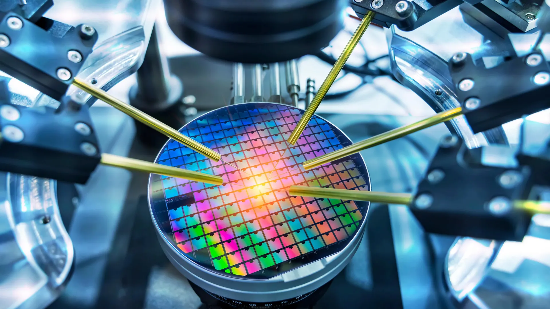
Microchips are fundamentally built on silicon wafers with intricate circuits etched onto their surface. This etching process relies on coating the wafer with a radiation-sensitive material - a ”resist” – and then using a radiation beam to burn the circuit patterns into the silicon. As manufacturers strive for ever-smaller features (currently around 10 nanometers), the radiation beams require increasing power. Though, traditional resist materials struggle to effectively interact with these higher-powered beams, hindering the precision and efficiency of the process.This translates to increased costs and limitations in performance.
“Companies are constantly looking ahead, planning their technology roadmaps for the next 10, 20 years and beyond,” explains Michael tsapatsis, a Bloomberg Distinguished Professor of chemical and biomolecular engineering at Johns Hopkins University and lead author of the study. “A major challenge has been identifying a viable process for creating these incredibly small features in a production environment – one that’s both precise and economically feasible.”
A New Approach: Metal-Organic Resists and Chemical Liquid Deposition
The Johns Hopkins team, building on previous work from Tsapatsis’s lab and the Fairbrother Research group, has pioneered a new class of resist materials based on metal-organics. These materials demonstrate a considerably stronger interaction with “beyond extreme ultraviolet radiation” (B-EUV) – a promising lithography technique poised to enable features smaller than the current 10-nanometer standard.
The key lies in the unique properties of these metal-organics. Metals like zinc effectively absorb the B-EUV light, generating electrons that trigger the necessary chemical transformations within an organic material called imidazole, ultimately imprinting the desired circuit patterns.
Crucially, the researchers have developed a novel method for depositing these materials onto silicon wafers with unprecedented control. This new methodology, termed chemical liquid deposition (CLD), allows for precise thickness control at the nanometer scale. This breakthrough was achieved through a collaborative effort involving researchers from Johns hopkins University, east China University of Science and Technology, École polytechnique Fédérale de Lausanne, soochow University, Brookhaven National Laboratory, and Lawrence Berkeley National Laboratory.
Unlocking a Universe of Material Combinations
“CLD is highly engineerable, allowing us to rapidly explore a vast landscape of metal and imidazole combinations,” Tsapatsis elaborates. “By carefully selecting these components, we can fine-tune the material’s ability to absorb light and facilitate the subsequent chemical reactions.”
The potential is enormous. With at least ten different metals and hundreds of organic compounds to choose from, the team is actively experimenting with various pairings to optimize performance for B-EUV radiation. This adaptability is notably significant, as the effectiveness of a material is wavelength-dependent.
“A metal that isn’t ideal for extreme ultraviolet radiation can be exceptionally well-suited for B-EUV,” Tsapatsis points out. “Zinc, for example, performs poorly with EUV but excels with B-EUV.”
Looking Ahead: manufacturing in the Next Decade
While the advanced lasers required for B-EUV lithography already exist, the development of these new materials and processes is the critical enabling step. The researchers anticipate that B-EUV technology, powered by these advancements, will be integrated into microchip manufacturing within the next 10 years.
This breakthrough represents a major step forward in the ongoing quest to push the boundaries of microchip technology, promising a future of increasingly powerful and efficient electronic devices.
Authors: Yurun Miao, kayley Waltz, and Xinpei Zhou from Johns Hopkins University; Liwei Zhuang, Shunyi Zheng, Yegui Zhou, and Heting Wang from East China University of Science and Technology; Mueed Ahmad and J. Anibal Boscoboinik from Brookhaven National Laboratory; Qi Liu from Soochow
Keep reading