For decades, the semiconductor industry has operated under the shadow of Moore’s Law—the observation that the number of transistors on a microchip doubles roughly every two years. However, as we approach the physical limits of silicon miniaturization, engineers are finding that shrinking components further is becoming an increasingly expensive and technically daunting challenge. In response, researchers are shifting their focus from horizontal scaling to a three-dimensional approach: stacking silicon chip layers to keep the pace of innovation alive.
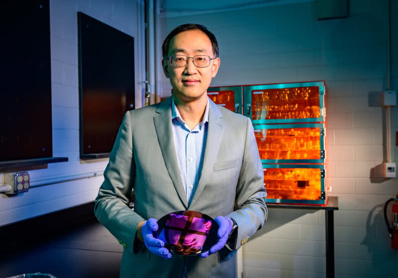
At the University of Illinois Urbana-Champaign’s Grainger College of Engineering, a team led by materials science and engineering professor Qing Cao has successfully developed a method for creating working silicon circuits by stacking active layers directly on top of one another. This move into the third dimension, often referred to as 3D integration, represents a significant departure from the traditional “system-on-a-chip” architecture that has defined modern computing for the last half-century. By building vertically, researchers hope to bypass the physical constraints that have begun to impede the performance gains of traditional planar transistors, as detailed in the official research report from the Grainger College of Engineering.
The End of the Road for Traditional Scaling
The core issue facing the industry is that as transistors reach the atomic scale, they begin to suffer from quantum mechanical effects, such as electron tunneling, which leads to increased power consumption and thermal instability. According to IEEE Spectrum, the industry has been grappling with these “short-channel effects” for years, forcing manufacturers to adopt complex manufacturing processes like FinFET and, more recently, Gate-All-Around (GAA) transistor architectures. These advancements have bought time, but the underlying physics remains a formidable adversary.
Professor Cao’s approach utilizes a technique that allows for the monolithic integration of these layers. Unlike traditional packaging, where separate chips are connected via wires, this method involves building active, functional circuitry on top of existing layers with high precision. This is not merely about stacking memory; It’s about creating a truly integrated, multi-story processor architecture. This technological shift is essential as the global demand for high-performance computing—driven by artificial intelligence and large-scale data processing—continues to outpace the capabilities of current flat-chip designs.
Overcoming Thermal and Manufacturing Barriers
Stacking chips is not a new concept, but doing it with high-performance silicon has historically been hindered by heat management and material compatibility. When you stack high-power components, the heat generated in the lower layers can degrade the performance of the layers above. To address this, the University of Illinois team focused on developing low-temperature fabrication processes that prevent the underlying circuitry from being damaged during the construction of the subsequent layers.

The research, published in the journal Nature Electronics, provides a blueprint for how these stacked layers can maintain structural integrity and electrical efficiency. As reported by the Nature Portfolio, the ability to maintain high carrier mobility—the speed at which electrons move through the material—is critical for ensuring that 3D-stacked circuits can compete with or outperform their 2D counterparts. This development is a crucial step toward realizing the promise of high-density, low-power electronics that could eventually power everything from mobile devices to massive server farms.
What This Means for the Future of Computing
If this technology can be scaled for commercial manufacturing, the implications for the tech industry are profound. First, it allows for a massive increase in transistor density without requiring the extreme ultraviolet (EUV) lithography advancements that currently cost billions of dollars to implement. Second, it reduces the physical distance signals must travel between logic and memory units, a phenomenon known as the “memory wall,” which is currently a primary bottleneck in processor performance.
For the average consumer, this could eventually translate to faster, more efficient devices that consume less battery power while handling the intensive workloads required by modern AI applications. However, the transition from lab-scale success to mass-market production is never immediate. The semiconductor manufacturing process is notoriously complex, and any new method must prove it can achieve high yields—producing thousands of identical, defect-free chips—to be economically viable for companies like TSMC, Intel, or Samsung.
Key Considerations for the Industry
- Thermal Management: Developing advanced cooling solutions for stacked silicon is essential as power densities rise.
- Interconnect Density: The ability to create high-speed, low-latency connections between layers is as important as the layers themselves.
- Cost Efficiency: The new fabrication methods must demonstrate a clear economic advantage over existing 2D scaling techniques.
Looking Ahead
As the industry looks toward the next decade, the focus will likely remain on refining these 3D integration techniques. The research conducted at the Grainger College of Engineering provides a vital proof-of-concept that demonstrates the feasibility of stacking active silicon layers. While we are not quite at the point where these chips will be inside our smartphones, the path forward is clearer than it has been in years.

The next major checkpoint for this technology will be the transition from experimental, single-stack prototypes to multi-layer wafers that can be tested for reliability under real-world operating conditions. Researchers are expected to present further findings at upcoming international conferences, such as the International Electron Devices Meeting (IEDM), where the industry evaluates the viability of emerging transistor technologies. We will continue to monitor these developments as they evolve from the research lab to the manufacturing floor.
What are your thoughts on the future of chip design? Do you believe 3D stacking will effectively replace current scaling methods, or will we see a hybrid approach? Share your insights and join the conversation in the comments section below.
Worth a look