
NVIDIA and its domestic partners are expanding semiconductor infrastructure and AI hardware production within the United States to bolster national supply chain resilience and accelerate domestic technological development. This multi-faceted initiative, which involves collaborations with major U.S. manufacturing firms and research institutions, aims to localize the production of high-performance computing components, including advanced GPUs essential for artificial intelligence workloads. According to official statements from the U.S. Department of Commerce, these efforts are increasingly aligned with broader federal goals to secure the domestic semiconductor ecosystem through the CHIPS and Science Act.
The Strategic Shift Toward Domestic Hardware Production
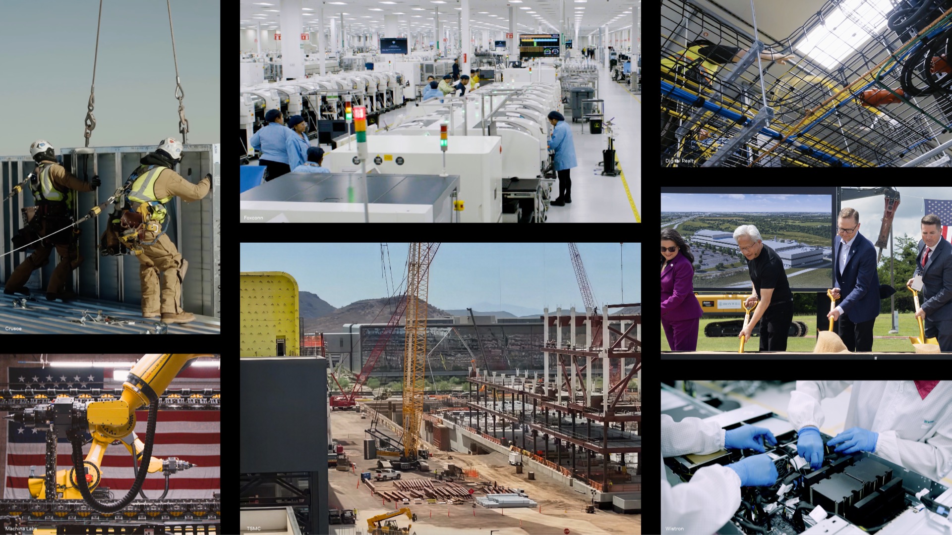
The push for “in America, for America” manufacturing represents a shift in how NVIDIA manages its global supply chain. For years, the company relied heavily on overseas foundries, particularly those in Taiwan. However, rising geopolitical tensions and the post-pandemic focus on supply chain security have prompted a pivot toward domestic production. NVIDIA CEO Jensen Huang has publicly noted the importance of a diverse and resilient supply chain, emphasizing that building capacity within the United States is a long-term strategic necessity for the American tech sector.

This transition is supported by federal funding mechanisms. Under the CHIPS and Science Act, the U.S. government has allocated billions of dollars in grants and loans to incentivize domestic semiconductor manufacturing. By partnering with major foundry operators and infrastructure providers in states such as Arizona, Ohio, and Texas, companies like NVIDIA are attempting to shorten the distance between hardware design and final assembly, thereby reducing the risks associated with international logistics and trade policy fluctuations.
Key Partnerships and Infrastructure Development
NVIDIA’s strategy relies on integrating its proprietary chip designs with the manufacturing capabilities of established U.S.-based or U.S.-operating partners. This includes working with firms that are currently scaling up their fabrication facilities to handle the complex, high-bandwidth requirements of modern AI processors. The integration of advanced packaging—a critical step in chip production—is a focal point of these domestic investments.
Beyond raw manufacturing, the initiative includes the development of regional AI data centers and research hubs. These facilities serve as testbeds for new hardware, allowing engineers to refine performance metrics in real-world environments. By keeping the R&D and manufacturing phases geographically closer, firms hope to shorten the feedback loop between hardware designers and the engineers managing production lines, a model often referred to as “co-location manufacturing.”
Why Domestic Semiconductor Production Matters
The primary driver for this localized approach is the stabilization of the supply chain for critical infrastructure. Modern AI models require thousands of interconnected GPUs, and any disruption in the supply of these components can delay the deployment of essential services in healthcare, defense, and finance. By fostering a robust domestic manufacturing base, the U.S. aims to mitigate the impact of external shocks.
Furthermore, the focus on domestic production is intended to spur regional economic growth. The construction of new, state-of-the-art semiconductor facilities requires thousands of high-skilled labor positions, ranging from software engineers and materials scientists to specialized equipment technicians. According to labor reports from the U.S. Bureau of Labor Statistics, the semiconductor manufacturing sector is currently a significant driver of high-wage job creation in regions seeing heavy investment.
Challenges in Scaling Domestic Capacity
Despite the momentum, significant hurdles remain. Building a semiconductor fabrication plant, or “fab,” is a capital-intensive process that can take several years to complete from groundbreaking to full production. Furthermore, the industry faces a well-documented talent gap, as there is a limited pool of personnel with the specific expertise required to operate the highly specialized lithography and packaging equipment necessary for next-generation AI chips.
NVIDIA and its partners are addressing these challenges through academic collaborations. By funding research programs at major universities and technical colleges, they aim to create a pipeline of qualified graduates ready to enter the workforce. These educational initiatives are vital, as the long-term success of the domestic manufacturing push depends on human capital as much as it does on physical infrastructure.
Future Developments and Policy Milestones
The next phase of this initiative involves the transition from construction to operational status for several major facilities currently under development. Stakeholders are closely monitoring the disbursement of remaining CHIPS Act funds, which are scheduled to be finalized in stages over the coming fiscal years. These financial milestones will dictate the pace at which new production lines come online.
Updates on the progress of these domestic facilities are expected to be provided during upcoming quarterly earnings calls and through official reports from the Department of Commerce. As these projects move toward completion, they will likely serve as benchmarks for the viability of large-scale, high-tech manufacturing within the United States. Readers interested in tracking the specific progress of these initiatives can find updates through the official portals of the companies involved and the White House briefing room for federal policy developments.
What are your thoughts on the shift toward domestic semiconductor production? Join the conversation below to share your perspective on how these changes might influence the future of global technology markets.