
In the high-stakes world of semiconductor manufacturing, the ability to diagnose defects with nanometer-level precision is no longer just an advantage—it is a requirement for maintaining yield. As integrated circuit architectures grow increasingly complex, failure analysis (FA) teams face the constant challenge of preparing samples that are both pristine and representative of real-world device conditions. A significant development in this field is the refinement of SEM-guided low-kV FIB finishing, a technique designed to balance the aggressive material removal of focused ion beams with the high-resolution imaging capabilities of scanning electron microscopes.
For materials scientists and yield engineers, the goal is to achieve “time-to-TEM” (Transmission Electron Microscopy) efficiency without compromising the structural integrity of the specimen. Modern workflows are moving toward integrated systems that allow for real-time visual feedback, effectively reducing the reliance on “blind” milling processes that historically led to sample damage or the need for costly rework. By utilizing advanced objective lenses and automated scan generators, these systems aim to provide the metrology-grade surfaces required for today’s leading-edge nodes.
Precision Engineering for Advanced Nanofabrication
The core challenge in failure analysis has long been the trade-off between speed and sample quality. Traditional Focused Ion Beam (FIB) milling often risks inducing artifacts or structural damage, particularly when working with delicate, thin-film materials common in modern transistors. To address these limitations, manufacturers have introduced systems that leverage a dual-beam approach: the FIB for material removal and the SEM for continuous, high-resolution monitoring. This “see while you mill” capability represents a shift toward more deterministic outcomes in nanofabrication.

By operating at low kilovolt (kV) levels, engineers can perform delicate polishing steps that minimize the interaction volume of the ion beam. What we have is particularly critical for preparing TEM lamellae, where the sample must be thin enough for electron transparency but robust enough to withstand handling. The integration of high-dynamic-range imaging allows for the suppression of background noise—often caused by the ion beam itself—enabling operators to observe the milling process with unprecedented clarity. This visual feedback loop is essential for precise endpointing, ensuring that the milling process stops exactly when the target feature is reached.
Optimizing Workflow Efficiency
For many semiconductor organizations, the ability to reduce turnaround time is directly tied to the “first-pass success” rate of sample preparation. When a sample is damaged during the milling process, the resulting data loss can set back yield improvement cycles by days or even weeks. Advanced FIB-SEM systems are designed to mitigate these delays by incorporating sophisticated scan generators that elevate image quality and process confidence. By reducing the need for iterative, manual adjustments, these systems allow teams to plan their turnaround times with greater reliability.
the move toward automated workflows helps standardize the output across different operators. In a global semiconductor environment, consistency is paramount. By automating the alignment and monitoring of the FIB process, labs can ensure that data-driven decisions are based on samples of uniform quality, regardless of the specific operator’s tenure or experience level. This is a critical step in scaling failure analysis operations to meet the demands of high-volume production environments.
The Future of Failure Analysis and Yield Management
As the industry pushes toward increasingly smaller geometries, the tools used for diagnostic analysis must evolve in tandem. The integration of SEM-guided low-kV FIB finishing is just one example of how the sector is adopting more sophisticated, automated methodologies. These advancements are not merely technical improvements; they are strategic investments in the speed and accuracy of the product development lifecycle. The ability to move from a raw sample to actionable insight with confidence remains the ultimate benchmark for any failure analysis lab.
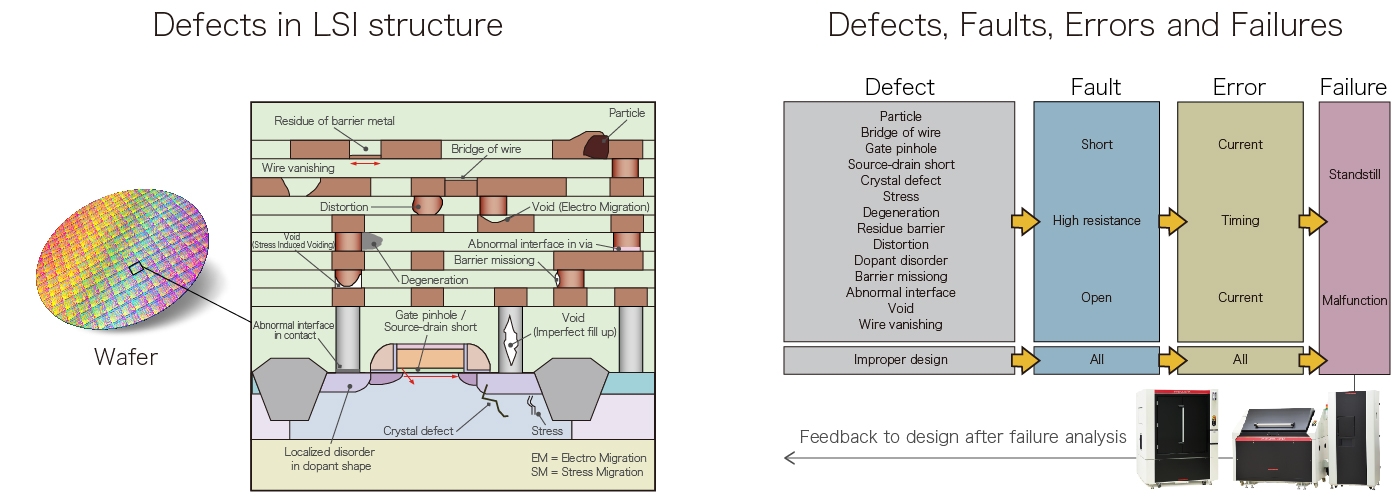
Looking ahead, the focus will likely remain on enhancing the synergy between ion and electron optics. As image acquisition times continue to drop, the potential for high-throughput tomography and automated lift-out procedures grows, promising a future where the bottleneck of physical sample preparation is significantly reduced. For now, the integration of these technologies serves as a vital bridge between the physical reality of the silicon wafer and the digital precision required to optimize it.
For those interested in the latest developments in semiconductor metrology and failure analysis, keep an eye on official industry conferences and technical journals, where manufacturers and research institutions regularly present new findings on ion-beam applications. We welcome your thoughts on how your own teams are navigating the challenges of modern device characterization. Please feel free to share your experiences or questions in the comments section below.
Worth a look