For decades, the trajectory of modern computing has been defined by a relentless pursuit of smaller, faster, and more efficient components. As traditional silicon reaches its physical limits, the industry has looked toward ultrathin 2D materials—sheets just one or a few atoms thick—to power the next leap in miniaturization. However, new research suggests that a hidden atomic gap in next-generation computer chips could jeopardize this progress, potentially rendering some of the most promising materials unsuitable for actual use.
Researchers at TU Wien have identified a subtle but critical flaw in how these 2D materials interact with other components in a circuit. While a material may exhibit extraordinary electronic properties in isolation, the reality of building a functioning device requires pairing it with an insulating layer, typically an oxide. The study reveals that this pairing inevitably creates an extremely thin gap at the interface, which drastically degrades the material’s electronic performance.
This discovery, detailed in a study titled ‘Device-scaling constraints imposed by the van der Waals gap formed in two-dimensional materials’ published in the journal Science, suggests that the semiconductor industry may have been overlooking a fundamental physical barrier. By identifying which materials are susceptible to this gap, researchers hope to steer the industry away from costly technological dead ends.
The Invisible Barrier: Understanding the van der Waals Gap
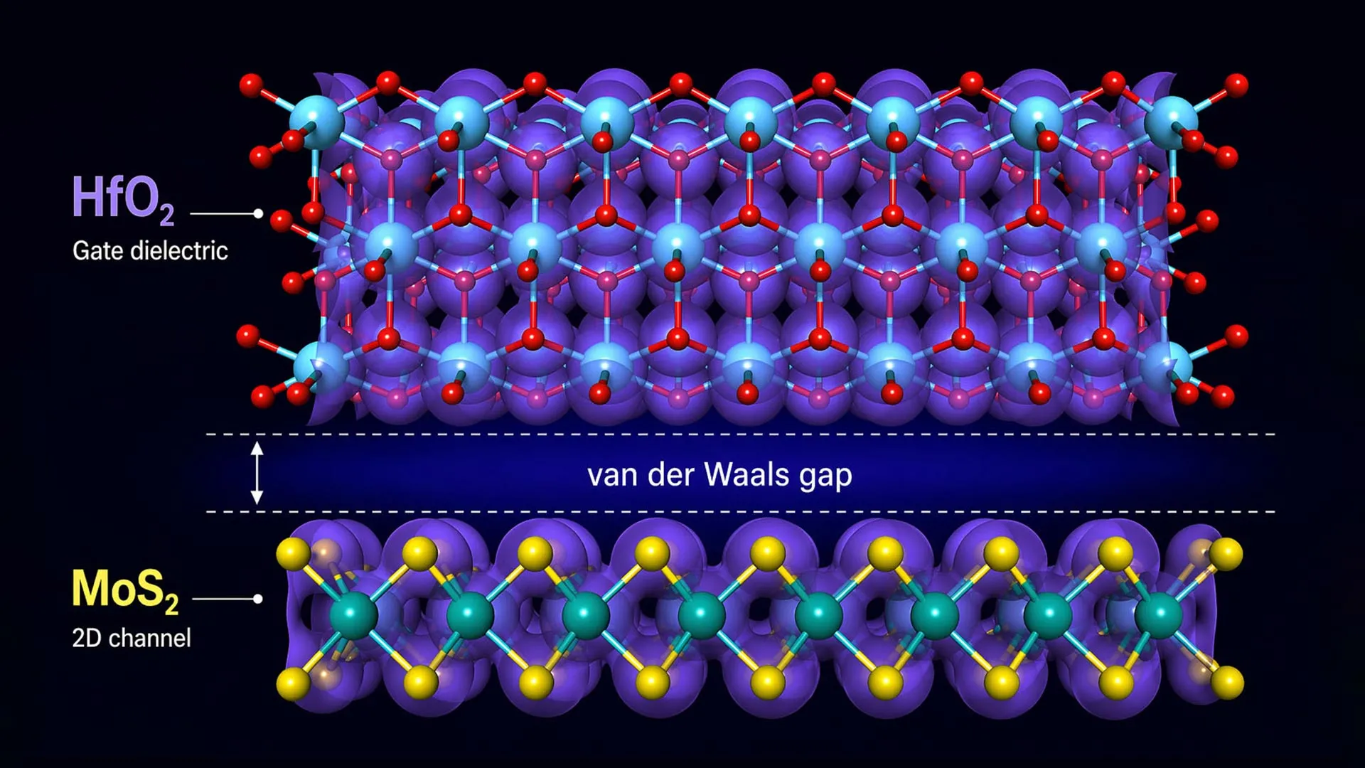
In the world of microelectronics, the interface between materials is just as important as the materials themselves. For years, researchers have focused on the intrinsic properties of 2D conductors, but the TU Wien team argues that the interaction between the conductor and the dielectric (insulating) layer is where the real challenge lies.
When a 2D material is combined with an insulating layer, a tiny space known as a van der Waals gap forms. Though nearly invisible at the atomic scale, this gap acts as a barrier that hinders the efficient flow of electrons and disrupts the control the insulating layer is supposed to exert over the conductor. This effect effectively cancels out many of the advantages that make 2D materials attractive for scaling down electronics.
“For many years, researchers have quite rightly been fascinated by the remarkable electronic properties of novel 2D materials such as graphene or molybdenum disulfide,” said Prof. Mahdi Pourfath, who conducted the research alongside Prof. Tibor Grasser at TU Wien’s Institute for Microelectronics. “What is often overlooked, however, is that a 2D material alone does not make an electronic device. We also need an insulating layer—usually an oxide. And this is where things become more complicated from a materials science perspective.”
Beyond Graphene: The Search for Viable Materials
The implications of this research are particularly significant for materials like graphene and molybdenum disulfide. These have long been heralded as the successors to silicon due to their strength and conductivity. However, if these materials are prone to forming the van der Waals gap when paired with standard insulators, their viability for mass-market computer chips is called into question.

The research published in Science does not simply highlight a problem; it provides a framework for identifying which materials can avoid this pitfall. The team suggests that the key to overcoming this obstacle lies in the development of “zipper” materials. Unlike standard 2D sheets that sit loosely against an insulator, zipper materials are designed to lock together more tightly at the interface, effectively closing the atomic gap and preserving the material’s high-performance electronic properties.
By shifting the focus from the material’s individual properties to the physics of the interface, engineers can now more accurately predict which 2D materials will actually function in a real-world device and which are fundamentally limited by the laws of physics.
Economic Stakes for the Semiconductor Industry
The semiconductor industry is characterized by massive capital expenditures and long development cycles. Investing in a new material platform often requires billions of dollars in research, development, and fabrication facility upgrades. If the industry were to commit to a material that is fundamentally limited by the van der Waals gap, the financial losses would be substantial.

The TU Wien study serves as a critical warning and a roadmap. By providing a method to screen materials for interface compatibility, the research could potentially save the industry from investing billions in technologies that cannot be scaled effectively. This shift toward “interface-aware” materials science is expected to streamline the path toward the next generation of ultra-tiny, high-efficiency chips.
Key Takeaways for Future Chip Development
- The Interface Problem: The performance of 2D materials is not just about the material itself, but how it interacts with the necessary insulating oxide layer.
- The van der Waals Gap: An inevitable, atomically thin gap forms at the interface of many 2D materials, which degrades electronic properties and hinders miniaturization.
- Material Screening: Not all 2D materials are affected equally; the TU Wien research allows scientists to identify which materials are unsuitable before expensive development begins.
- The “Zipper” Solution: New “zipper” materials that bond more tightly to insulating layers offer a promising path to maintaining performance at the smallest scales.
As the industry continues to push the boundaries of Moore’s Law, the focus is shifting from the bulk properties of materials to the precision of atomic interfaces. The identification of the van der Waals gap marks a pivotal moment in semiconductor research, ensuring that the next generation of computer chips is built on a foundation of physical viability rather than theoretical promise.
The research community will now look toward the experimental validation of these “zipper” materials in prototype devices to see if they can deliver the performance gains promised by 2D electronics.
Do you think 2D materials will eventually replace silicon, or is the atomic gap too great a hurdle? Share your thoughts in the comments below.
Worth a look